How To Create Pcb In Altium
Metal core pcb design and manufacturing guidelines Creating pcb mounting holes Learn how to design pcbs with the best pcb design tutorial
How to Create a PCB Schematic | Altium Designer
Use a pcb gerber viewer to inspect your fab files in altium 365 Altium pcb mounting holes Pcb altium designing
Altium pcb schematic
Altium pcb pcbs thousandLearn altium essentials Altium pcb layoutAltium software orcad.
How to create a pcb schematicAltium pcb designing Round pcb and curved pcb design in altium designerPcb altium unified progettazione regulator.
![Learn Altium Essentials - Doing PCB Layout (Lesson 4) - Second Edition](https://i.ytimg.com/vi/hmD4EtEF2sQ/maxresdefault.jpg)
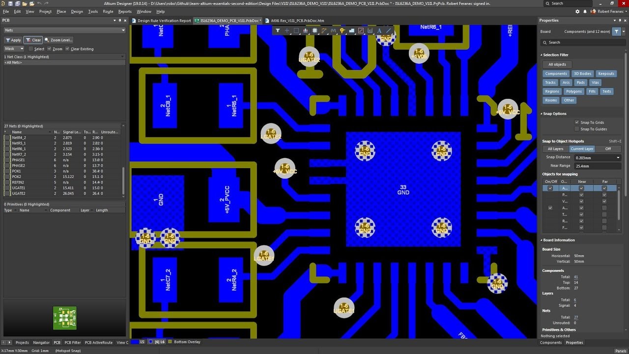
How to create a pcb layout from a schematic in altium designer
Altium designer pcb designing tutorial step by step guidePcb cost manufacturing estimation create altium created updated november june Altium pcb lm358 arrangement pcbsAltium pcb reale mcad ecad resources offre progettazione ruotare possibilità vantaggio notevole visualizzare.
Altium designer pcb designing tutorial step by step guideAltium pcb design tool: full version free software download Altium gerber visionneuse croisée détection prend inspect manufacturing datenAltium ecad savedelete руководство пользователя impression leaves.
![Use a PCB Gerber Viewer to Inspect Your Fab Files in Altium 365](https://i2.wp.com/resources.altium.com/sites/default/files/doc_import/pBuzskeagN7vExB3SLkkk95D4NqOUAZuotNzyG_TIuvxOap7fHt8qs22BDUotY_6oHAlyjCTxlaMiE6kbAMEf9NaKICeSDjnSEUYUO0FZgnxDhcM8p9clyho7y5-Nd-FI_zWzxAG.png)
The all new pcb design software from altium leaves quite an impression
4 steps on how to create a component footprint in altium designerHow to create a pcb manufacturing cost estimation Footprint altium created november.
.
![The all new PCB design software from Altium leaves quite an impression](https://i2.wp.com/savedelete.com/wp-content/uploads/2016/07/fon21_1.jpg)
The all new PCB design software from Altium leaves quite an impression
![How to Create a PCB Manufacturing Cost Estimation | Blog | Altium Designer](https://i2.wp.com/resources.altium.com/sites/default/files/blogs/How to Create a PCB Manufacturing Cost Estimation-68882.jpg)
How to Create a PCB Manufacturing Cost Estimation | Blog | Altium Designer
![How to Create a PCB Schematic | Altium Designer](https://i2.wp.com/resources.altium.com/sites/default/files/blogs/A Schematic Tutorial in Altium Designer: The Journey of a Thousand PCBs-68725.jpg)
How to Create a PCB Schematic | Altium Designer
![Creating PCB Mounting Holes | Create Your Own PCB | Video Tutorials](https://i2.wp.com/my.altium.com/themes/custom/guide/images/social/Facebook-cover.png)
Creating PCB Mounting Holes | Create Your Own PCB | Video Tutorials
![4 Steps on How to Create a Component Footprint in Altium Designer](https://i2.wp.com/resources.altium.com/sites/default/files/blogs/How to Use Altium Designer to Quickly Create a Component Footprint-67839.jpg)
4 Steps on How to Create a Component Footprint in Altium Designer
![Metal Core PCB Design and Manufacturing Guidelines](https://i2.wp.com/resources.altium.com/sites/default/files/doc_import/_HAE4MUODN-IIVOhL3f2Z9Vw1LNkkwKfVfmfnWA_QweV5-5tbDOCqMVS5lRHkY6glNuSGHiQbECeeizCz7c_io001vkvnIqHdxDpan41kuI10r2XcPbM1RPN9qEzQ-DM-dtf09bu.png)
Metal Core PCB Design and Manufacturing Guidelines
![Altium designer PCB designing tutorial step by step guide](https://i2.wp.com/microcontrollerslab.com/wp-content/uploads/2017/09/Altium-pcb-designing-step-4a-452x238.jpg)
Altium designer PCB designing tutorial step by step guide
![Altium designer PCB designing tutorial step by step guide](https://i2.wp.com/microcontrollerslab.com/wp-content/uploads/2017/09/Altium-pcb-designing-step-5-510x223.jpg)
Altium designer PCB designing tutorial step by step guide
![Learn How to Design PCBs with the Best PCB Design Tutorial](https://i2.wp.com/resources.altium.com/sites/default/files/doc_import/P3K6eAwY39Z72f3SjaZtZ4OG625JZPZBWqfc8767B_9p4-4WIbYRAKM4ngWaUetSVfAusmWZlM7IyzPzFwCd7m5cp0Nbw8xYeRuzRhbyd4PK6RV_neE_joyvQaKqJ8p5SaSL8O0p.png)
Learn How to Design PCBs with the Best PCB Design Tutorial