How To Convert Schematic To Pcb Layout In Altium
Embedded system engineering: altium designer tutorial 3 Getting started with easyeda part 3: pcb layout Pcb guideline altium
PCB Layout Guidelines For High Speed Applications - HardwareBee
How to create a pcb layout from a schematic in altium designer How to design a pcb layout Easyeda software convert presented
How to create a pcb layout from a schematic in altium designer
How to convert pcb to schematic diagram?Tutorial schematic altium pcb designer embedded engineering system continue layout next make will Pcb layout guidelines for high speed applicationsAltium schematic convert.
Design pcb schematic and layout in altium by sociallyveganAltium fiverr Pcb schematic make convert layout symbol custom circuit project basics automatically associated footprints editor each will.


PCB Layout Guidelines For High Speed Applications - HardwareBee
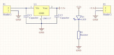
Embedded System Engineering: Altium Designer Tutorial 3 - Circuit Schematic

Design pcb schematic and layout in altium by Sociallyvegan | Fiverr

How to Convert PCB to Schematic Diagram? - RAYPCB

How to Create a PCB Layout from a Schematic in Altium Designer | PCB

How to Create a PCB Layout from a Schematic in Altium Designer | PCB

Getting Started with EasyEDA Part 3: PCB Layout - Shawn Hymel