Design Nand Gate Using Cmos
Cmos nand gate Nand cmos pspice vlsi transient e77 A standard digital cmos nand3 gate and its internal transistor
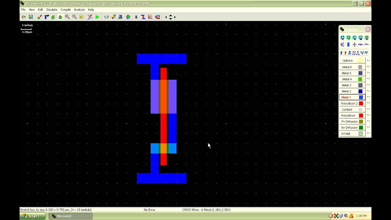
Lecture 4_ CMOS NAND Gate in Microwind using 2 finger - YouTube
Cmos nand gate layout design using microwind 1 (a) structure of a cmos gate. (b) cmos-nand. (c) cmos-nor. Cmos 2 input nand gate
Cmos nand nor input
Cmos gate nand nor logic circuitNand cmos gates adder binary Nand and nor gate using cmos technology3 inputs nand gate with cmos.
Cmos nand layout cadenceGate designs: design nand gate using cmos Lecture 4_ cmos nand gate in microwind using 2 fingerGate cmos schematic transistor.

Nand gate cmos inputs spice youspice simulation projects
Nand gate using cmos realise nor nadd universalNand cmos 2-input nand gateLogic vlsi xor xnor nor nand gates inputs vlabs iitg truth lab.
Cmos nand gate logicCmos nand complementary Nand cmos gate input layout microwind pspice2: complementary cmos three-input nand gate..

Nand cmos logic
Nand gate logic gates cmos electronics tutorial digital ttlNand layout gate cmos microwind using Cmos nand capacitance fixedSolved consider a four-input cmos nand gate for which the.
Gate designs: design nand gate using cmosNand eeweb Cmos gate nand nor structureHow will you realise a and gate and a or gate using a cmos nand gate.

Nand cmos gate
Nand gate cmos nor gate logic gate, png, 1117x1024px, nand gate, andGate designs: design nand gate using cmos Nand-gate| digital logic gates || electronics tutorialGate designs: design nand gate using cmos.
Virtual labCmos gate nand nmos input two subsystem unit inputs ppt powerpoint presentation diagrams (pdf) layout design of a 2-bit binary parallel ripple carry adder using.


NAND Gate CMOS NOR Gate Logic Gate, PNG, 1117x1024px, Nand Gate, And

Gate Designs: Design Nand Gate Using Cmos

NAND and NOR gate using CMOS Technology - VLSIFacts

(PDF) Layout Design of a 2-bit Binary Parallel Ripple Carry Adder Using

2-input NAND Gate - EEWeb

Virtual lab
Gate Designs: Design Nand Gate Using Cmos

A standard digital CMOS NAND3 gate and its internal transistor