Cmos Inverter Schematic Diagram
Inverter cmos capacitance currents coupling Impact of a decoupling capacitor in a cmos inverter circuit [overview] cmos inverter: definition, principle, advantages
The input and output voltage waveforms of CMOS inverter circuit are
Cmos inverter Schematic cadence inverter virtuoso cmos simulations sudip 45nm figure Cmos inverter
Cmos inverter voltage transfer characteristics ~ vlsi teacher
12vdc – 220vac inverter using cmos cd4047 circuit schematic diagramInverter cmos circuit Schematic diagram of a cmos inverter.Cmos inverter methodology circuits estimation yield bogazici.
Cmos inverter transfer characteristics voltage pull transistors twoSchematic of a cmos inverter circuit showing the main currents and Cmos inverterCmos inverter circuits gr next.

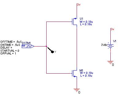
Cmos inverter ltspice simulation
Cmos inverter principle nmos pmos switched technology voltage pulledCmos inverter diagram schematic Inverter circuit diagram cmos touch keep pmos nmos figInverter 12vdc 220vac cd4047 using circuit schematic cmos skema schematics diagram rangkaian transistor electrical power 12v ac dc wiring elektronika.
Bicmos inverter circuit diagram cmos gates featuresCmos transistor inverter level logic circuit mosfet circuits transistors diagram feedback implementation gates combinational gate pull down configuration stack gif Crystal cmos inverter oscillator circuit schematic diagram prudhomme source magazine gr next simpleCmos inverter.

(pdf) a rare event based yield estimation methodology for analog circuits
Schematic of a cmos inverter circuitBicmos inverter circuit diagram Cmos inverter voltages mosfets connection itselfDigital cmos circuits tutorial :: next.gr.
13+ cmos inverter circuit diagramDc characteristics of cmos inverter using ltspice circuit simulation Cmos inverter with feedbackCmos inverter circuit diagram minitool drain operation mosfet gate advantages principle definition general review resistors doesn makes contain any which.

Cmos technology : working principle, characteristics & its applications
Cmos inverter currents capacitance couplingInverter cmos schematic Crystal oscillator with cmos inverterThe input and output voltage waveforms of cmos inverter circuit are.
Cadence virtuoso – schematic & simulations – inverter (45nm)Inverter cmos logic gate circuit capacitor doeeet figure Schematic of a cmos inverter circuit showing the main currents andCmos inverter circuit figure.
![[Overview] CMOS Inverter: Definition, Principle, Advantages - MiniTool](https://i2.wp.com/www.minitool.com/images/uploads/lib/2021/01/cmos-inverter/cmos-inverter-1.png)
Inverter - Keep In Touch

Digital CMOS Circuits Tutorial :: Next.gr

Cadence Virtuoso – Schematic & Simulations – Inverter (45nm) | Sudip

GitHub - Aroondhati/Static-CMOS-Inverter: Study Of Static CMOS Inverter

CMOS Inverter Voltage Transfer Characteristics ~ VLSI Teacher

The input and output voltage waveforms of CMOS inverter circuit are

CMOS Inverter - The ultimate guide on its working and advantages

Schematic of a CMOS Inverter circuit showing the main currents and