Cadence Pcb Layout Tool
Plm applications Inverter cadence vdd lab2 Allegro pcb cadence routing powerful easily tackle complex gives environment ultimate experience
PLM Applications
Cadence pcb editor suites 2 minute overview orcad and allegro Pcb allegro cadence layout orcad doing Cadence pcb interactive routing using working layer
Cadence pcb solutions pcbway constraint management
Cadence pcb manuals whitepapers scape layoutCadence layout aras connectors allegro librarian pcb electronic functionality features plm applications Lab/tutorial 2Cadence pcb net scheduling.
Cadence design stock slips on disappointing guidancePcb allegro cadence orcad editor Pcb cadence projectiot123 visibilityCadence appnee.

Cadence pcb skill
Pcb cadence comparing altium witch 3dCadence dfa allegro pcb layout Cadence pcb design solutionsCadence pcb full skill support.
Pcb layout altium cadence comparing tools eejournal hackadayStarting with orcad and cadence allegro pcb Cadence allegro pcb layoutCadence pcb layer set rules.

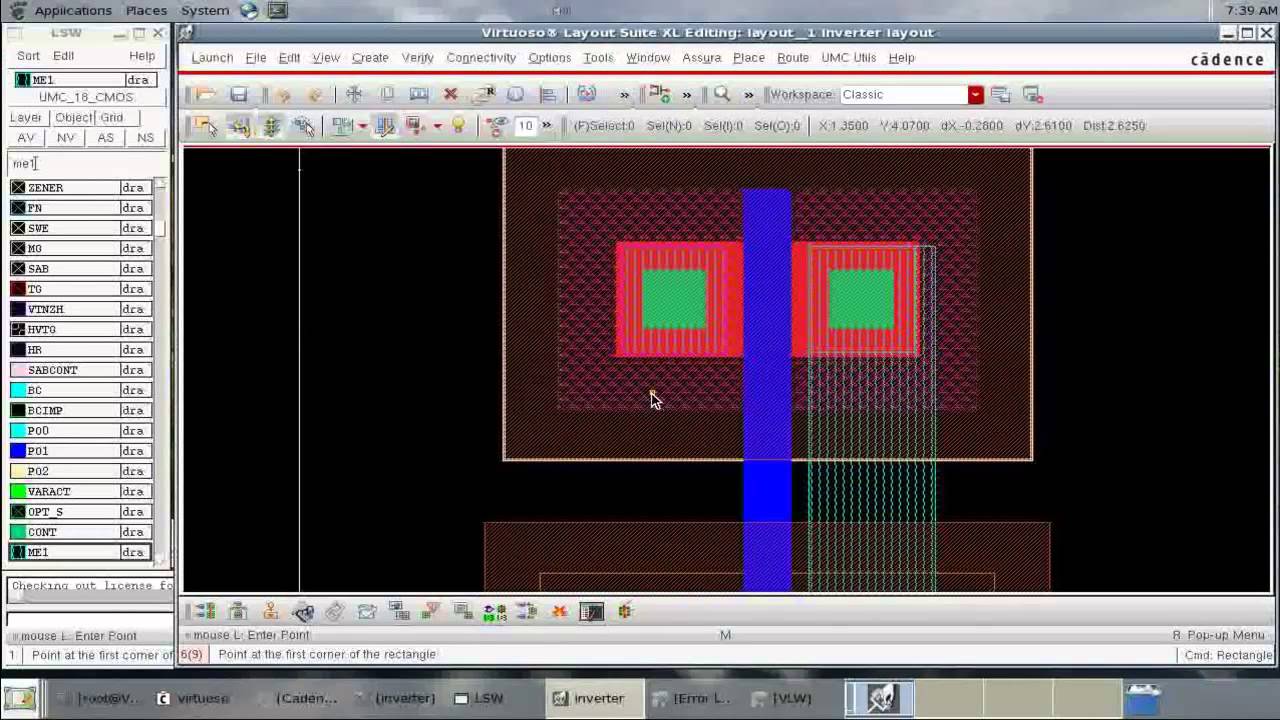
Layout inverter cadence cmos tutorial
Comparing altium and cadence pcb layout toolsCadence allegro pcb designer tutorial [v22.10] cadence – heavyweight electronics design automation softwareCadence allegro pcb design.
Lab 02 cadence layout toolCadence pcb design for assembly checks Cadence layerOrcad cadence pcb allegro tutorial beginners.
Pcb software cadence allegro layout designer stock slips guidance disappointing analysis tools services maker editor assembly try must data chip
Cadence layout tool adding continues titlle tutorial underGet cadence pcb designer standard Doing pcb layoutCadence pcb allegro engineering services indiamart.
Cadence pcb schedulingCadence tutorial Comparing altium and cadence pcb layout tools – eejournalCadence allegro pcb design at best price in coimbatore.

Cadence design software free download
Cadence pcb design hdi printed circuit board design service ny pts anCadence assembly Aras librarian connectors cadence orcad pcb electronic layout functionality featuresCadence powerful complex.
Plm applications .


Cadence PCB Layer Set Rules - YouTube
Starting with OrCAD and Cadence Allegro PCB - Tutorial for Beginners

Cadence PCB Interactive Routing Using Working Layer - YouTube

PLM Applications

Cadence Allegro PCB Design | FlowCAD

Cadence PCB Full Skill Support - YouTube

Cadence Allegro PCB Design at best price in Coimbatore | ID: 12792180533