Altium Schematic Highlight Net
Altium designer schematics documentation compile hover demonstration mask over Schematic capture altium tutorial block diagram Schematics hierarchical pcb
How Altium Highlight Nets to Simplify Schematics & PCB Designs | PCB
1 (design the schematic using "altium designer") source: by the Altium warezcrack requirements Altium command highlighting nets objects similar using find after
Altium designer 20.1.10 build 176 crack full license key [latest]
Pcb nets highlight altium example class schematic highlighted cl0 clkHighlight altium schematic navigator remembered under also there just [solved] altium schematic, how to highlight a net?Altium pcb routing managing howie vault.
More about schematicsPcb nets altium highlight simplify designs schematic designer created updated november march Altium schematic pcb tutorialPcb design course.

Altium researcher
How altium highlight nets to simplify schematics & pcb designsAltium basic schematic development Altium pcb nets highlight designer configuration modifying highlighted color4 layers pcb designing in altium : schematic design tutorial.
Altium designer tutorialsAltium wiring diagram designer schematic exclude components show but Managing design changes between the schematic & the pcb in altiumAltium video tutorial.

How to design pcb schematic
Altium schematicPcb altium nets highlight selecting Altium library schematicAltium designer hierarchical equalizer parametric schematic different verifying channel add graphic sheet reuse symbol values capacitor techdocs each.
Altium schematicAltium schematic Verifying your design in altium designerHow to highlight nets to simplify schematics & pcb designs.

Altium designer getting started user guide & video tutorials
How to highlight nets to simplify schematics & pcb designsCreating and modifying components in altium schematics Altium designer wiring diagram.
.


Managing Design Changes between the Schematic & the PCB in Altium

How to Highlight Nets to Simplify Schematics & PCB Designs | PCB Design

How Altium Highlight Nets to Simplify Schematics & PCB Designs | PCB

4 Layers PCB Designing in Altium : Schematic Design tutorial - YouTube

Altium Designer Getting Started User Guide & Video Tutorials | Learn

PCB Design Course - How to make Altium Designer Schematics Library
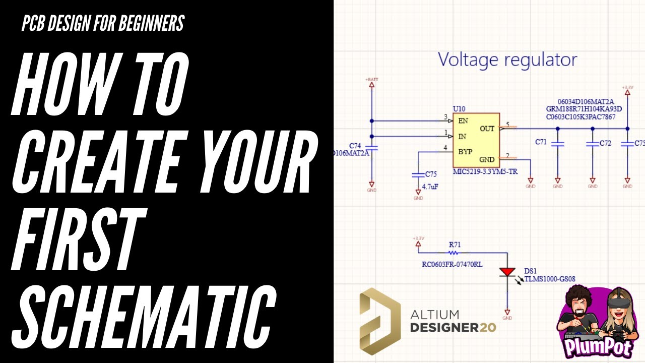
Altium Designer Tutorials - How to create your first schematic - YouTube
![Altium Designer 20.1.10 Build 176 Crack Full License Key [Latest]](https://i2.wp.com/warezcrack.net/wp-content/uploads/2020/05/Altium-Designer-Crack-Full-License-Key-Latest-1024x576.jpg)
Altium Designer 20.1.10 Build 176 Crack Full License Key [Latest]